
ASML: Next-gen chipmaking tool ready for production in 2016
There are two big hurdles to continuing Moore’s Law, the observation that over the long run transistor density doubles approximately every two years producing systems that are cheaper and more capable. The first is that as things get smaller, it is harder to maintain the same level of performance and reliability. The industry has addressed this problem with a series of innovations in materials and structures, most recently with the introduction of 3D transistors of FinFETs. The second is that, even if you do figure out how to make such small transistors work, you may not be able to “print them” on a wafer because current lithography tools are running out of steam. For now, the industry is using an expensive stopgap, called multi-patterning, but ultimately what it really needs is a new tool and the leading candidate is known as EUV (Extreme Ultra-Violet) lithography.
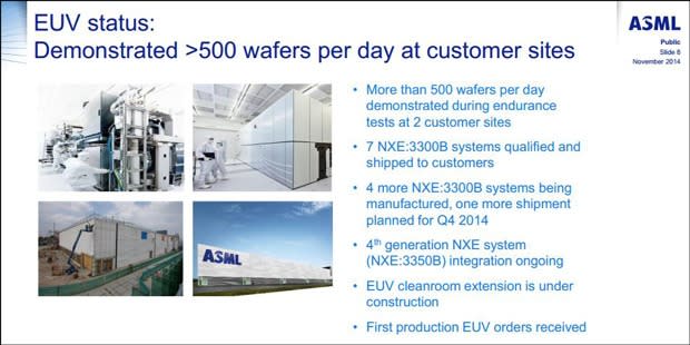
ASML, one of the world’s largest suppliers of chipmaking equipment, is the only company actively developing EUV systems (Nikon has fallen behind). Earlier today, during an investor day in London, ASML gave an update on its progress on increasing the power of the light source, and therefore the throughput, of EUV to make it competitive with the existing Deep UV (DUV) scanners. ASML has already shipped seven of its current EUV too, the NXE:3300B, and it said that multiple customers have been running it with a source power of 80 watts, which is sufficient to process about 500 wafers per day. ASML said it has a roadmap to reach 125 watts and 1,000 wafers per day next year and 250 watts and 1,500 wafers per day—the level required for real volume manufacturing—in 2016.
ASML also announced that one of its key customers, contract chipmaker Taiwan Semiconductor Manufacturing Corp. (TSMC), has ordered two NXE:3350B EUV systems for delivery in 2015 “with the intention to use them in production.” TSMC is also planning to upgrade its two NXE:3300B systems to deliver the same performance.
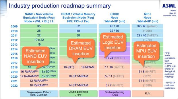
If ASML is successful, it believes that some foundry customers (TSMC, Samsung and GlobalFoundries) could start using EUV to pattern a few critical layers at the 10nm node starting in 2016. The current DUV scanners, which use light with a wavelength of 193nm, have to make several passes to pattern features this small, so EUV can be more competitive because it uses light with a wavelength of only 13.5nm and can handle this geometry with one or two passes.
Intel has already said EUV won’t be ready in time for its 10nm node, and during its own investor day last week, the company said it could continue to increase transistor density and reduce cost at 7nm even without EUV. But ASML still believes that Intel will use EUV for 7nm production starting around 2018. In memory, EUV will be used first for DRAM manufacturing around 2017 followed by NAND flash memory in 2018-2019 (the current shift from planar to 3D NAND has bought the industry some time).
Of course there are other issues aside from source power and EUV has missed many deadlines over the years. It first started showing up in roadmaps in the 1990s and at one point was expected to replace 193nm scanners to manufacture chips below 100nm (with a possible interim stop at 157nm that never materialized). CNET News reported in 2001 that EUV would debut in 2005 at 70nm or chipmaking would simply “grind to a halt.” Instead the industry came up with some new tricks--including immersion lithography, which uses a liquid between the lens and wafer surface rather than air to enhance the resolution, and more recently multi-patterning—to extend things and today Intel is manufacturing 14nm processors using the same 193nm light.
But chipmaking is growing more complex and expensive, and ASML says EUV litho is now a matter of “when, not if.” So perhaps this time will really be it. ASML said that if things go as planned, it expects to ship 50 to 60 EUV systems per year by 2020, generating more than $12 billion in revenue.
John Morris is a former executive editor at CNET Networks and senior editor at PC Magazine. He now works for a private investment firm, which may at any time invest in companies whose products are discussed in this blog, and no disclosure of securities transactions will be made. No investment advice is offered in this blog. All duties are disclaimed.
